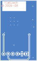
A test board with an ESP32-C3 module and a 3D-printable enclosure. Schematic, board, checks and enclosure are all generated by scripts. The enclosure's dimensions are not read off a drawing but from the board's 3D model, so it fits the connector and the LED.
The board is exported from KiCad with its components, copper and silkscreen; the enclosure and lid are the exact parts that go to the printer. The slider pulls the parts apart.
This is a test board from the FlatLock project, not the board the lock runs on today. It has not been manufactured or printed yet; what is verified and what is not is listed below.
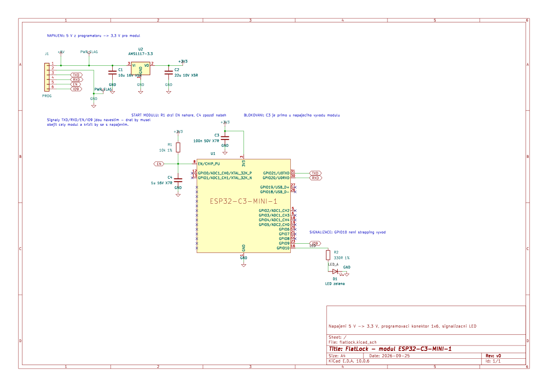
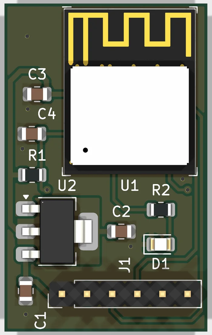
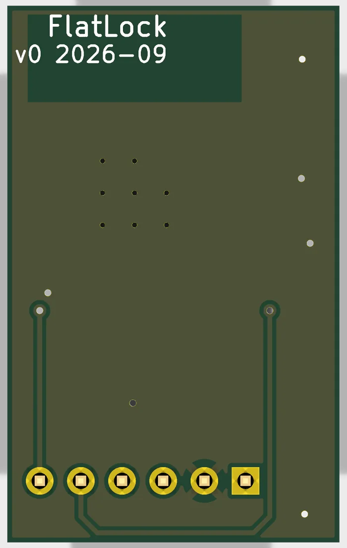
Schematic, component placement, routing, the board in 3D and the enclosure step by step.
Full video
Short, under a minute
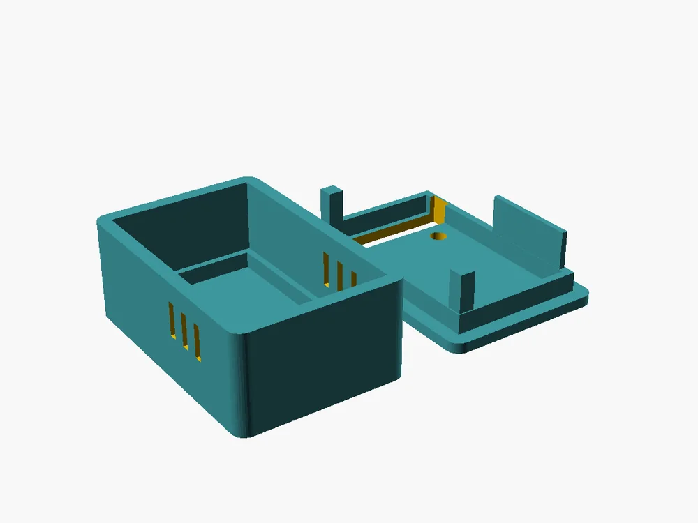
The board has no mounting holes, to keep it as small as possible. So the enclosure holds it differently: the board rests on a ledge around the edge and posts on the lid press it down from above. Every dimension is derived from the board.
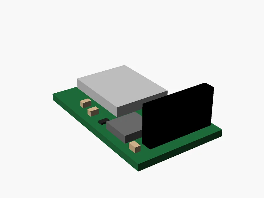
Outline and component bodies from the board's 3D model. The ESP32-C3 module came out 2.39 mm tall; the datasheet says 2.4.
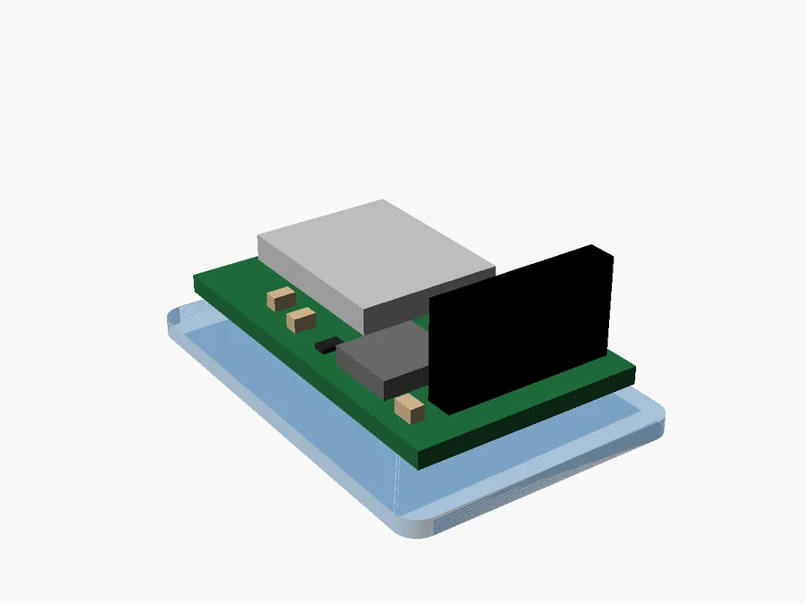
1.6 mm with rounded corners. 0.4 mm clearance around the board on every side.
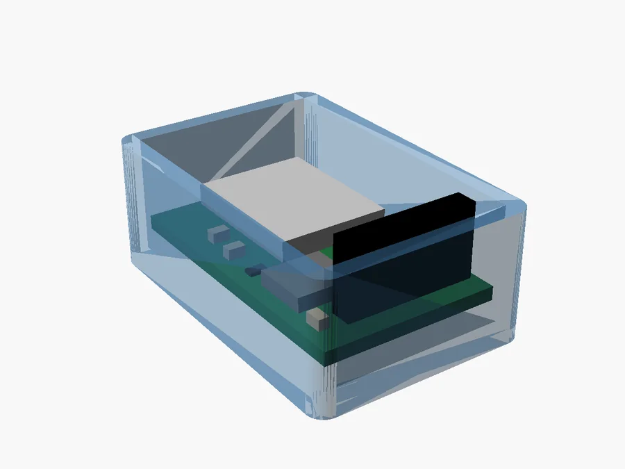
Height is set by the tallest part: the J1 header stands 8.5 mm above the board, plus 0.5 mm margin.
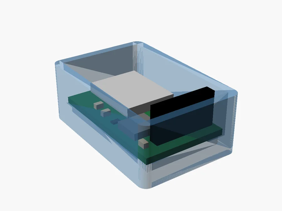
J1 pins stick out 1.4 mm below the board, so the ledge holds it 2.4 mm above the base. A check makes sure it runs under no pin.
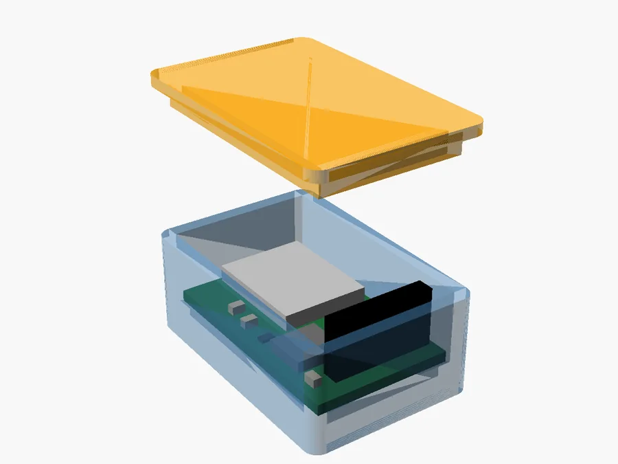
A 3 mm lip drops into the box with 0.2 mm clearance, to be tuned on the first print.
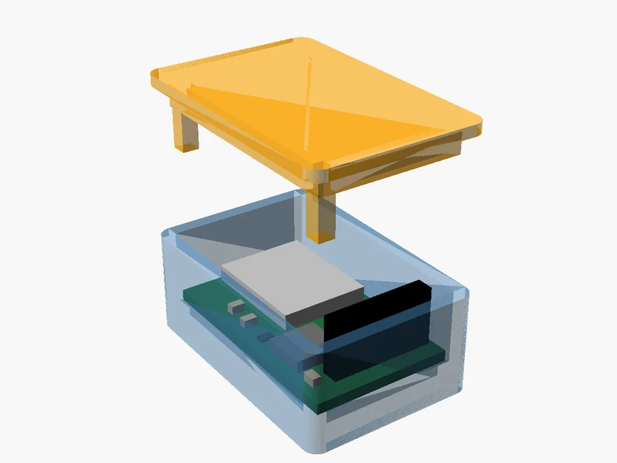
Posts only in corners with nothing in the way: two of four qualified. A rib along the right edge, where 1.25 mm is left between the module and the edge.
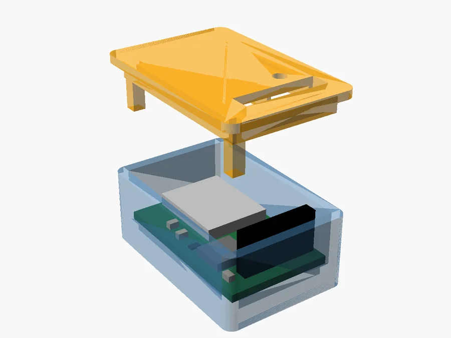
An opening right above J1 with 0.6 mm clearance for the cable connector, a 2.6 mm window above LED D1. Positions taken from the board.
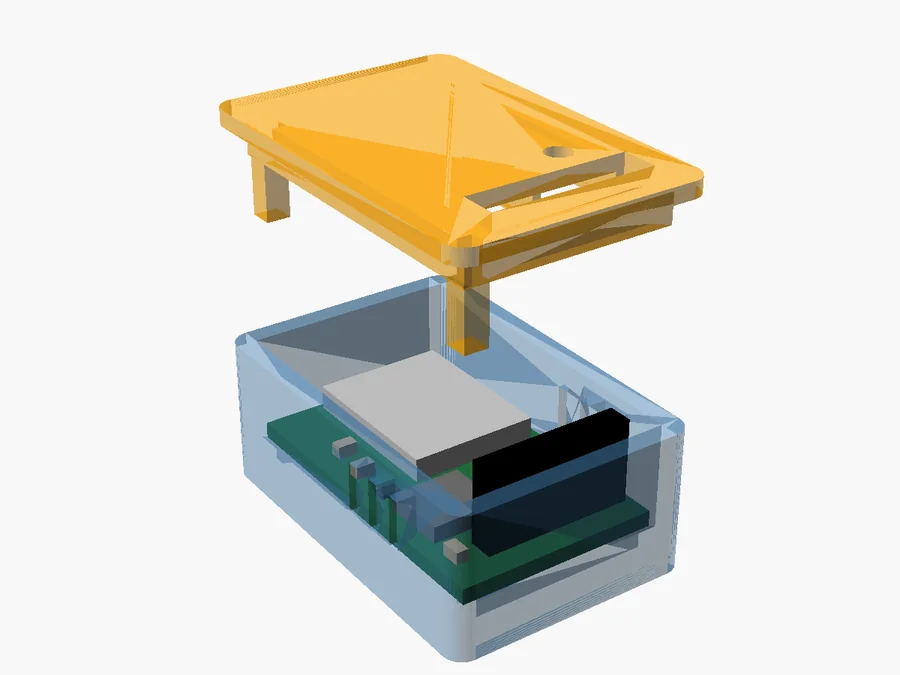
Three slots in each long wall next to the regulator, which dissipates 0.58 W at peak.
On the previous board, component positions were copied into the enclosure model by hand and ended up 10 mm off. Here no number is copied. When the board changes, the enclosure is recomputed with one command.
Placed according to the schematic's netlist.
kicad-cli exports it including the package models.
A script reads the board outline and a box around each component.
OpenSCAD derives the dimensions and stops on anything that would collide.
Print-ready parts, the step images and the 3D model above.
Why from the 3D model and not the board drawing: the package outline in the drawing is an assembly courtyard with an allowance, not the real body, and it has no height at all. The opening in the lid and the gap above the board need the actual body.
Drawn as a document, not as a list of connections: power and functional blocks are drawn as wires; labels remain only where a wire would have to go around the whole module. After writing it, the script has KiCad export the netlist and compares it with the expected nets.
| Pin | Signal |
|---|---|
| 1 | 5 V |
| 2 | GND |
| 3 | TXD (module output) |
| 4 | RXD (module input) |
| 5 | EN (reset) |
| 6 | IO9 (boot) |
One cable both powers and programs the board. The LED is on GPIO10 because GPIO2, 8 and 9 decide the boot mode at startup and an LED to ground could pull them low.
Two layers, 20.5 x 33.1 mm. The size follows the content, not a guess: the width is set by a corridor of two traces right of the module, the height by the module on top and a trace under the header. Ground is not routed; it is a copper pour on both sides. There is no copper under the module's antenna, verified with 35 samples on both layers.
These numbers are not estimates. A script computes them directly from the finished board, so they cannot drift from the design.
The peak is the module transmitting over Wi-Fi. The module figures are commonly quoted values for now, not from the datasheet.
Per IPC-2221 (18 µm copper), 0.134 mm is enough for 344 mA. Half a millimetre is therefore not about heating but about voltage drop and lower inductance.
| State | Loss | Die, 25 °C ambient |
|---|---|---|
| idle, 109 mA | 0,19 W | 36 °C |
| peak, 344 mA | 0,58 W | 61 °C |
| peak, no copper under the tab | 0,58 W | 95 °C |
The junction limit is 125 °C. About 1 cm² of copper under the tab is therefore a necessity, not decoration.
| Where | Loop | Inductance | |
|---|---|---|---|
| C3 100n | module supply | 5,0 mm | 2,0 nH |
| C4 1u | module EN | 6,1 mm | 2,4 nH |
| C2 22u | regulator output | 4,8 mm | 1,9 nH |
| C1 10u | regulator input | 5,5 mm | 2,2 nH |
What matters is the area of the current loop, not the distance from the pin. Each capacitor therefore has its own ground via right next to its pad.
Manufacturing is designed for the fab's cheapest standard spec: construction class 5, narrowest trace 0.30 mm, clearance 0.25 mm, drill 0.30 mm. No surcharges.
Send me your KiCad board. The enclosure is computed from its 3D model and you get STL files for printing plus images for your documentation. Or we start from the schematic.
Send an emailDavid Petrov · davidpetrov@email.cz